
Transparent PCB: A New Choice for Future Electronic Designs
Transparent PCBs (Printed Circuit Boards) are gradually becoming an essential innovation in the electronics industry due to their unique appearance and outstanding performance. With the continuous advancement of technology, transparent PCBs are showing immense potential in various fields, including smart devices, automotive electronics, medical equipment, and more. This article will provide a comprehensive analysis of transparent PCBs, including their definition, common materials, manufacturing process, advantages, challenges, and future applications, helping you understand this innovative technology and its wide-ranging value.
What is a Transparent PCB?
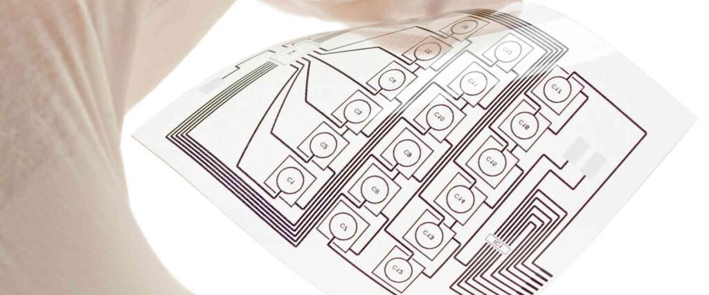
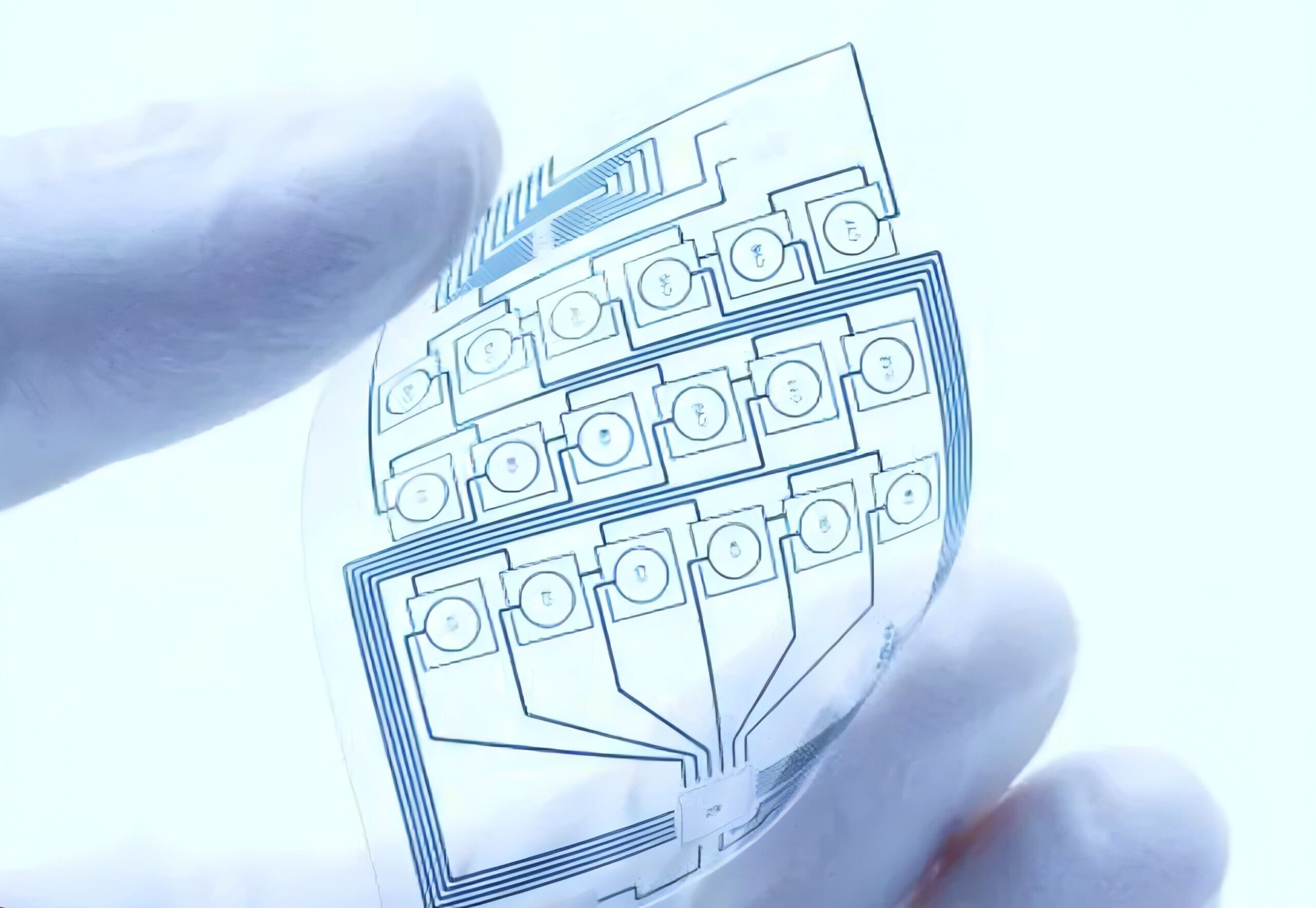
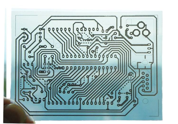
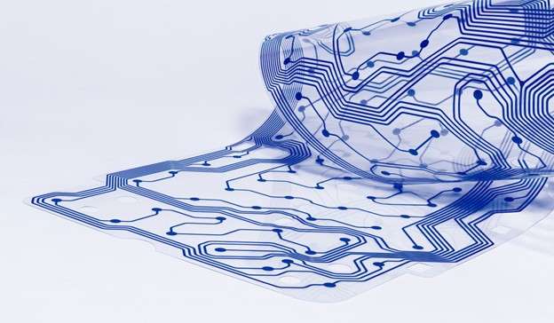
A transparent PCB is a type of printed circuit board made from transparent or semi-transparent materials. These boards offer the same electrical performance as traditional PCBs but with the added benefit of a unique visual effect that allows for more creative design possibilities. Transparent PCBs are widely used in devices that require aesthetic appeal, such as smart devices, LED displays, automotive interiors, and more. Compared to conventional PCBs, transparent PCBs provide significant advantages in terms of visual appeal and design flexibility.
Moreover, transparent PCBs are not just visually attractive; they also provide reliable electrical connections and stable performance. Thus, transparent PCBs not only enhance product appearance but also ensure the proper functioning of electronic devices.
Common Materials Used in Transparent PCBs and Their Characteristics
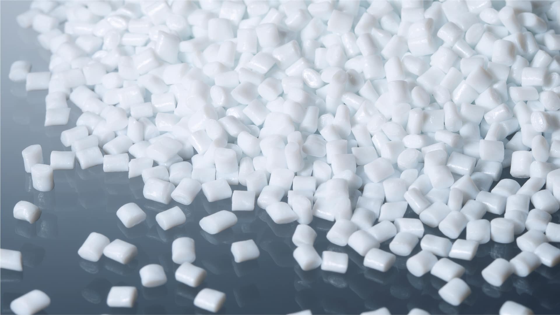
The key to transparent PCBs lies in the selection of materials. Transparency, conductivity, mechanical strength, and heat resistance are the primary considerations when choosing the appropriate material. Here are several common materials used in transparent PCBs and their characteristics:
1. Polycarbonate (PC)
Known for excellent transparency and impact resistance, making it ideal for applications that require high strength, such as automotive electronics and consumer electronics products.
Good high-temperature resistance, suitable for high-temperature environments.
2. PET (Polyethylene Terephthalate)
Offers excellent transparency and flexibility, making it the material of choice for flexible transparent PCBs.
Strong chemical resistance, widely used in electronic products that require lightweight and high transparency.
3. PMMA (Polymethyl Methacrylate)
Has extremely high light transmission and is commonly used in applications such as LED displays and backlighting.
Easy to process, suitable for precision displays and transparent electronic components.
4. Glass-reinforced epoxy Resin (GER)
By adding glass fibers to epoxy resin, it enhances mechanical strength and stability.
Commonly used in transparent PCBs that require higher rigidity and durability.
5. Liquid Crystal Polymer (LCP)
Excellent heat resistance and dimensional stability, make it ideal for high-performance transparent PCBs.
Its electrical properties and thermal stability make it suitable for high-end electronic products.
The selection of different materials determines the application areas and performance of transparent PCBs. Therefore, choosing the appropriate material according to the specific product requirements is crucial.
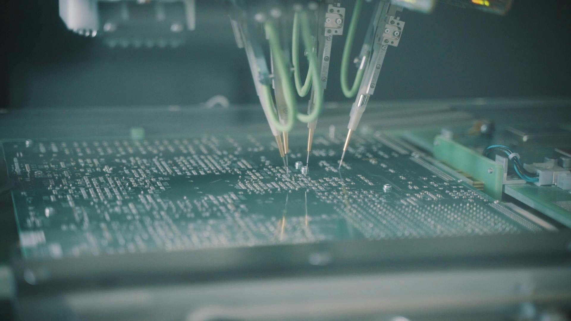
Manufacturing Process of Transparent PCBs
The manufacturing process of transparent PCBs is more complex than traditional PCBs, as it needs to ensure both electrical performance and material transparency. The main steps in the transparent PCB manufacturing process are as follows:
1. Substrate Preparation
The manufacturing process of transparent PCBs begins with selecting the right substrate, which is then cleaned and treated to ensure its surface is free of contamination and compatible with subsequent processes.
2. Metallization
A metal layer is deposited on the surface of the transparent substrate using chemical or physical methods to form the electrical circuit connections. This step is critical for transparent PCBs, and it requires special care to ensure that the metalization does not affect the transparency of the material.
3. Imaging and Etching
Photolithography is used to transfer the circuit pattern onto the substrate, followed by an etching process to remove unwanted metal, forming the circuit design.
4. Drilling and Plating
The PCB is drilled to create holes for interlayer connections and component insertion. After drilling, plating is performed to ensure electrical connectivity in the holes.
5. Solder Mask and Silkscreen Printing
A transparent solder mask ink is applied to protect the surface of the PCB, and text or markings are printed. The transparent solder mask effectively prevents the PCB from moisture or oxidation while preserving its visual integrity.
6. Routing and Cutting
After fine-cutting and routing, the transparent PCB is shaped into the required form and is ready for the assembly process.
7. Testing and Inspection
Once the transparent PCB is completed, it undergoes rigorous functional testing and visual inspection to ensure that both its electrical performance and aesthetic qualities meet the requirements.
Due to the complex processes involved, the production of transparent PCBs requires high precision and strict control to ensure that each step does not compromise the material’s transparency.
Advantages and Challenges of Transparent PCBs
Advantages:
- Aesthetic Appeal
Transparent PCBs provide a unique visual effect that can enhance the design of a product, especially in devices that showcase internal circuitry or have high aesthetic demands.
- Creative Design Flexibility
The use of transparent PCBs breaks the limitations of traditional circuit board designs, offering designers greater creative freedom, especially in fields like smart devices and automotive electronics, where technology and art need to be combined.
- High Reliability and Stability
Like traditional PCBs, transparent PCBs offer excellent electrical connection properties and mechanical strength, making them suitable for high-end electronic products.
- Versatility
Transparent PCBs are not only suitable for standard electronic applications but can also be used in flexible PCB designs, expanding their range of applications.
Challenges:
- Complex Manufacturing Process
The production of transparent PCBs requires extremely high process precision. Every manufacturing step must be carefully controlled to avoid affecting the material’s transparency, and the limited choice of materials further increases the complexity of production.
- High Cost
Due to the expensive materials used and the complex manufacturing process, the overall cost of transparent PCBs is higher than that of traditional PCBs. Therefore, transparent PCBs are typically used in high-end products.
- Balancing Transparency and Electrical Performance
Maintaining transparency while ensuring electrical performance, especially in multi-layer designs, presents significant technical challenges.
Applications of Transparent PCBs
The wide range of applications of transparent PCBs makes them an innovative choice across multiple industries:
- Consumer Electronics
Transparent PCBs are widely used in smartwatches, transparent displays, and wearable devices, providing endless creative possibilities for product design while balancing aesthetics and functionality.
- Automotive Electronics
Transparent PCBs are utilized in automotive interiors, transparent displays, and lighting systems, enhancing the overall aesthetic of the car while maintaining high reliability in electrical performance.
- Medical Equipment
Transparent PCBs are used in high-end medical devices for display modules and instrument panels, providing clear visibility while ensuring the stability and durability of the equipment.
- Smart Home and Other Sectors
Transparent PCBs are also used in smart home devices, IoT products, and more, offering high transparency and performance, making them the top choice for designers and engineers.
The Future of Transparent PCBs
As the technology for transparent PCBs continues to improve, their potential for applications in various industries will only expand. In the future, transparent PCBs are expected to combine with flexible PCBs, creating even more innovative applications. With advances in material technology, the production cost of transparent PCBs is expected to gradually decrease, making them more accessible for a broader range of applications.
Transparent PCBs not only represent a new trend in electronic product design but also drive the advancement of electronic manufacturing technology. As more companies and designers turn their attention to this technology, transparent PCBs are poised to occupy a more significant position in the future of the electronics industry.
Conclusion and Collaboration Suggestions
Transparent PCBs, as an emerging electronic design solution, are leading the future of electronic product design due to their unique advantages. As a professional PCB manufacturer, JY PCBA is committed to providing high-quality transparent PCB solutions for our clients. With our extensive production experience and advanced manufacturing processes, we can meet various client needs in the field of transparent PCBs.
If you are looking to incorporate innovative elements into your product design, enhancing both visual appeal and functionality, please feel free to contact us. We will provide you with customized transparent PCB solutions to help drive your product innovation and market success.