
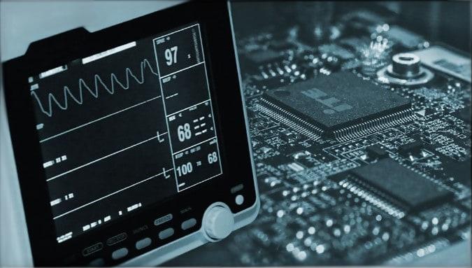
Printed Circuit Boards (PCBs) are the backbone of modern electronics, enabling the functionality of everything from smartphones to medical devices. But how does a custom PCB go from an idea to a fully functional product? This article walks you through the step-by-step process, from design and prototyping to fabrication and assembly.
1. Concept and Requirements Definition
Every great PCB starts with a clear understanding of the project’s goals. Engineers and designers work together to define:
- Functionality: What will the PCB do?
- Size constraints: How big or small should it be?
- Power requirements: Voltage, current, and power consumption
- Signal integrity: High-frequency vs. low-frequency considerations
- Environmental factors: Will it be exposed to heat, moisture, or vibration?
At this stage, designers may also choose between a single-layer, double-layer, or multi-layer PCB based on complexity.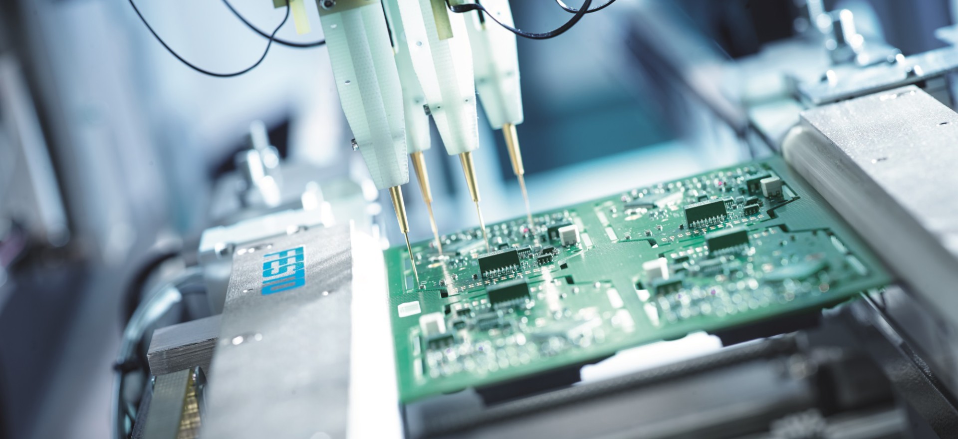
2. Schematic Design
Using specialized Electronic Design Automation (EDA) software like Altium Designer, KiCad, or Eagle, engineers create a schematic diagram. This is essentially a blueprint that shows how all electronic components are connected.
Key steps include:
- Selecting appropriate components (resistors, capacitors, ICs, connectors, etc.)
- Defining electrical connections and signals
- Assigning reference designators for each part
- Running simulations to ensure circuit functionality
3. PCB Layout and Routing
Once the schematic is finalized, it’s time to lay out the PCB. This involves:
- Placing components in an optimized manner
- Defining trace widths and spacing
- Creating power and ground planes for stability
- Routing signal paths to minimize interference
For high-speed PCBs, additional considerations like impedance control and differential pair routing are applied.
4. Prototype Fabrication
Before mass production, a prototype PCB is manufactured for testing. This includes:
- Selecting a PCB substrate (FR4, Rogers, etc.)
- Choosing a surface finish (HASL, ENIG, OSP, etc.)
- Fabricating the board using processes like photolithography, etching, and drilling
A small batch of prototype boards is produced for testing.
5. PCB Assembly (PCBA)
With the prototype in hand, it’s time to mount components onto the PCB. This involves:
- Solder Paste Application: Applying solder paste to pads where components will be placed
- Pick and Place: Automated machines place components onto the board
- Reflow Soldering: The board passes through a reflow oven to solder surface-mount components
- Through-Hole Soldering: Hand or wave soldering for through-hole components

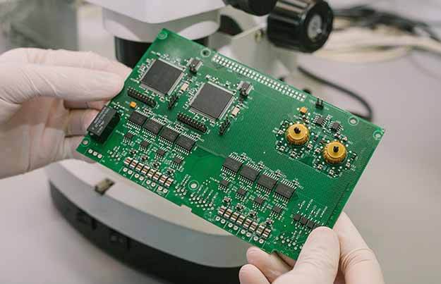
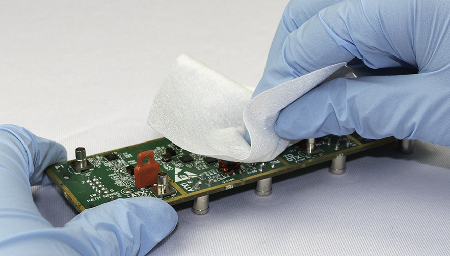
6. Testing and Quality Control
Before a PCB is ready for production, it undergoes rigorous testing:
- Automated Optical Inspection (AOI): Scans the board for defects
- X-ray Inspection: Used for BGA and hidden solder joints
- Functional Testing: Ensuring the PCB performs as intended
- In-Circuit Testing (ICT): Checking individual components
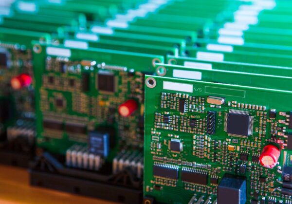
7. Mass Production and Final Assembly
Once the prototype passes all tests, the PCB moves to full-scale production. This includes:
- Large batch fabrication
- Assembly and soldering at scale
- Final product integration
At this stage, additional protective coatings and heat sinks may be applied to improve durability.
8. Packaging and Shipping
The final PCBs are packaged according to customer specifications and shipped to manufacturers or end-users.
The journey from concept to a fully functional PCB is complex but essential for modern electronics. By following a structured process—design, layout, prototyping, testing, and mass production—engineers ensure that PCBs meet high-performance and reliability standards. Whether for consumer gadgets or industrial machinery, every PCB plays a crucial role in making technology work!