

Multilayer PCBs
In the design and manufacturing of modern electronic products, multilayer PCBs (Printed Circuit Boards) play a crucial role. By stacking multiple conductive layers, they meet the demands of high-density and high-complexity circuit designs. This article will delve into the definition, working principle, advantages, and application fields of multilayer PCBs, and provide guidance on how to choose the right manufacturer, helping you better understand the role and potential of multilayer PCBs in the electronics industry.
What is a Multilayer PCB?
A multilayer PCB is a circuit board made by combining two or more conductive copper layers with insulating material layers through lamination technology. Compared to traditional single-sided or double-sided PCBs, multilayer PCBs offer greater circuit integration capabilities. Their basic structure consists of at least three or more conductive copper layers, which are interconnected by vias to ensure the stability of the circuit and the smooth transmission of signals.
Multilayer PCBs are not only suitable for high-density integrated circuit designs but also meet the strict requirements for size, weight, and performance. Therefore, many modern electronic products, such as smartphones, computers, and industrial control devices, extensively use multilayer PCB technology.
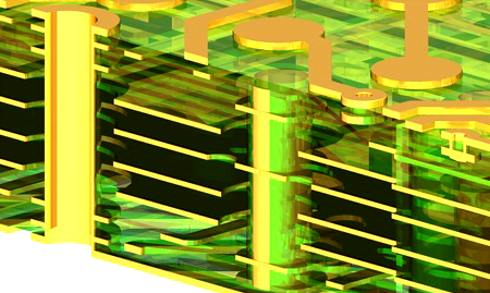
Working Principle of Multilayer PCBs
The working principle of a multilayer PCB is closely related to its structure. Each conductive layer is connected through vias, and there are different types of vias, each playing a different role in the circuit board:
Through-Hole Vias: Vias that pass through the entire circuit board, commonly used to connect signals or power between different layers.
Blind Vias: Vias that only connect the outer layers with one internal layer, leaving other layers unconnected. These are used to increase circuit density.
Buried Vias: Vias that only exist between internal layers and are not connected to the outer layers, typically used in high-density designs to save space on the outer layers.
These vias provide a pathway for signal transmission in the circuit, ensuring proper flow of current or signals between layers. Additionally, the signal transmission quality in multilayer PCBs benefits from reduced electromagnetic interference, optimized current paths, and improved system performance through proper layout.
Advantages of Multilayer PCBs
Multilayer PCBs have several obvious advantages over traditional single-sided and double-sided PCBs. Whether in terms of physical performance, electronic performance, or manufacturing advantages, they bring significant value to customers.
Physical Advantages
Smaller Size: The stacked structure of multilayer PCBs makes circuits more compact, enabling the integration of more functions within a limited space. This is crucial for miniaturized consumer electronics, such as smartphones and tablets.
Lighter Weight: By reducing the use of components and materials through more compact wiring and integration, multilayer PCBs help reduce the overall weight of the device. This is important for portable devices and wearable electronics.

Performance Advantages
High Quality and Powerful Functionality: The structure of multilayer PCBs allows for more complex circuit designs while providing higher performance and stronger functionality, meeting the demands for high frequencies, high speeds, and low latency.
Increased Durability: The conductive layers and insulating material layers in multilayer designs enhance the durability of the circuit boards, especially against temperature variations, moisture, and mechanical vibrations, making them suitable for harsh environments.
Enhanced Design Flexibility: Due to the complex design of multilayer PCBs, they can integrate more functions, such as multiple signal transmissions, power and ground layers, making designs more flexible and adaptable to complex application requirements.
Single Connection Points: By reducing the number of connection points, multilayer PCBs minimize connection issues, which is particularly important for high-frequency applications to avoid signal distortion and interference.
Manufacturing Advantages
Higher Assembly Density: Through stacking multiple conductive layers, multilayer PCBs enable more functions to be integrated within a smaller area, making them ideal for complex circuit designs requiring high-density connections.
Support for Complex Circuit Designs: Multilayer PCBs can support more complex circuit designs, such as high-frequency circuits, precision sensors, and power management systems, which require higher circuit integration and stronger signal transmission capabilities.
Typical Application Fields of Multilayer PCBs
As multilayer PCB technology has developed, its applications have become increasingly widespread. From consumer electronics to military defense, and from medical to industrial control fields, multilayer PCBs are used in nearly all high-end electronic devices. Below are some typical application areas:
Consumer Electronics
In consumer electronics such as smartphones, tablets, and laptops, multilayer PCBs serve as the foundation for high-performance and compact designs. They integrate more functions while maintaining a small form factor.

Telecommunications
Communication equipment such as base station devices and communication modules rely on multilayer PCBs for stable signal transmission and high-frequency performance, supporting faster data transfer and more efficient network infrastructure.
Medical Devices
In the medical industry, devices like imaging systems and monitoring equipment require high precision and reliability in their circuits. Multilayer PCBs ensure high-quality signal transmission, meeting the strict demands of medical equipment.

Industrial Control
For systems like automated production lines and control panels, multilayer PCBs support complex circuits and high-frequency operations, ensuring efficient and reliable equipment performance.
How to Choose a Multilayer PCB Manufacturer?

Choosing the right multilayer PCB manufacturer is critical to the success of your project. Here are several important factors to consider when selecting a PCB manufacturer:
Production Capability
Does the manufacturer have the capacity to handle complex designs and large-scale production? Ensure they can manage high layer counts, various sizes, and special materials.
Cost Optimization
A good PCB manufacturer should have the ability to control costs effectively, providing competitive prices without compromising quality, ensuring that the project stays within budget.
Quality Assurance
Quality is the core of multilayer PCB production. The manufacturer should have a rigorous quality control system, including automated optical inspection (AOI), in-circuit testing (ICT), X-ray inspection, and more, ensuring that every PCB meets the required standards.
Customization Support

The manufacturer should offer customized services based on customer requirements, including prototype development, flexible solutions, and quick turnaround for special needs.
Conclusion and Call for Collaboration
Multilayer PCBs, with their exceptional circuit design capabilities, are widely used in various high-end electronic products. Their advantages not only lie in their miniaturization and reduced weight but also in their performance and manufacturing advantages, supporting the development of modern technology. JY PCBA, with its advanced technology and extensive experience, is committed to providing high-quality multilayer PCBs and flexible solutions tailored to customer needs. We invite clients from various industries to collaborate with us to jointly drive innovation in electronic products.
For more information or to request a quote, please feel free to contact us. We are dedicated to serving you.
Appendix: Technical Capabilities Overview of Multilayer PCBs
| PCB Capacity | Capability |
| Layer Count | 1-24 layers |
| Maximum Panel Size | 558×670 mm |
| Minimum Board Thickness | 4 layers: 0.40 mm, 6 layers: 0.80 mm, 8 layers: 1.00 mm, 10 layers: 1.20 mm |
| Minimum Line Width/Spacing | 0.065 mm |
| Minimum Finished Hole Size | 0.10 mm |
| Hole Wall Copper Thickness | Max 35 microns |
| Maximum Copper Thickness in Patterns | 210 microns |
| PTH Hole Diameter Tolerance | 0.05 mm |
| NPTH Hole Diameter Tolerance | 0.025 mm |
| Aspect Ratio | 10:1 |
| Hole Position Accuracy | Min +/0.05 mm |