
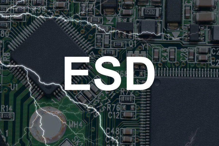
PCB Electrostatic Discharge (ESD) Guide: A Comprehensive Protection Strategy from Design to Manufacturing
In the modern electronics industry, electrostatic discharge (ESD) is an important issue that should not be overlooked. For PCBs and electronic components, ESD can cause serious performance problems or even complete failure. To ensure product quality and reliability, it is essential to have a full understanding of the sources, impacts, and effective protection measures for ESD. This article will comprehensively explore the hazards of ESD and provide a detailed protection strategy that covers everything from design to manufacturing.

What is Electrostatic Discharge (ESD)?
Electrostatic discharge (ESD) refers to the sudden flow of electricity between two objects with different electrical charges. This phenomenon does not require a specific voltage; as long as there is a sufficient voltage difference and a short enough distance between the two objects, ESD can occur. ESD often happens silently, but it carries a huge potential for damage.
ESD can have the following impacts on PCBs and electronic components:
- Soft Failures: Performance degradation occurs, but the device can still operate. These subtle issues are often difficult to detect and can have long-term effects on the product.
- Potential Defects: Components may appear normal on the surface, but internal performance is already compromised, leading to a shorter lifespan and increased risk of failure.
- Catastrophic Failures: ESD can instantly destroy components, causing the product to fail completely and become non-functional.

The destructive potential of ESD should not be underestimated, especially for precision electronic devices, where its impact can be fatal.
Sources of Static Electricity
Static electricity primarily originates from friction and contact between different materials. When materials with opposite charges come into contact and then separate, they can accumulate static electricity. Here are some common scenarios where static electricity can build up:
Rapid Airflow
For example, fans or compressed air devices can generate static electricity due to high-speed friction with surfaces.
Contact with Synthetic Materials
Materials such as foam packaging or plastic bags are common sources of static electricity. If not properly controlled during production or transportation, they can easily trigger ESD.
Use of Ungrounded Equipment
If portable tools or mobile devices are not grounded properly, they increase the risk of ESD.
In addition to the scenarios above, static electricity tends to accumulate more easily in low humidity environments. This is particularly true during the dry autumn and winter seasons, where the static charge is harder to dissipate.
Specific Impact of ESD on PCBs
The impact of ESD on PCBs is more severe than one might think. Its effects include the following:
1. Overheating and Component Burnout
ESD can cause a sudden surge of current, which results in overheating. High temperatures can directly damage the internal structure of components, making them non-functional. This damage is often irreversible, especially for high-frequency circuits and sensitive components.

2. Ionization of Conductors and Current Pulses
ESD can cause the ionization of conductors, generating short-duration, high-intensity current pulses. These pulses can travel through PCB tracks or even through the air to strike components, resulting in burned solder joints, damaged tracks, and irreparable damage.
3. Susceptibility of Integrated Circuits and Connectors
Integrated circuits (ICs) and connectors are particularly vulnerable to ESD. Even small electrical discharges can render these components non-functional, causing the entire circuit to fail.

ESD Protection Design Strategy
To mitigate the risks of ESD on PCBs, effective protection measures should be implemented at both the circuit design and PCB layout levels.
Circuit Design-Level Protection
- Grounding Layer Design
Adding a grounding layer can significantly reduce parasitic inductance in the circuit, improving overall circuit stability and helping to protect it from static electricity. A proper grounding design enhances the circuit’s ability to dissipate any electrostatic charges and reduces the likelihood of ESD damage.
- Increasing Conductor Spacing
Sufficient spacing between conductors is crucial to prevent electrical breakdown or leakage. This is especially important in high-voltage circuits where closer spacing can lead to arcing. Ensuring adequate creepage and clearance distances will help protect the circuit from electrical surges.
- Protection at Input/Output Ports
Transient voltage suppressors (TVS) or surge protection diodes should be installed at input/output ports to absorb high-voltage pulses, providing extra protection for the circuit. This will safeguard sensitive components from sudden electrical spikes.
- Optimizing IC Pin Layout
Avoid placing vulnerable parts of the circuit, such as sensitive IC pins, in locations where they could be easily affected by ESD. Properly routing traces and using vias in critical areas can help minimize the risk of electrostatic damage.
Optimizing PCB Layout
- Reducing Impedance
By shortening the paths between radiation sources and pulse generators, you can reduce the impedance, minimizing the risk of ESD and electromagnetic interference (EMI).
- Proper Grounding Design
Implementing multi-point grounding and vias in the PCB design helps to ensure a low-impedance path for ESD dissipation. This provides a direct route for electrostatic charges to be safely discharged, protecting sensitive components.
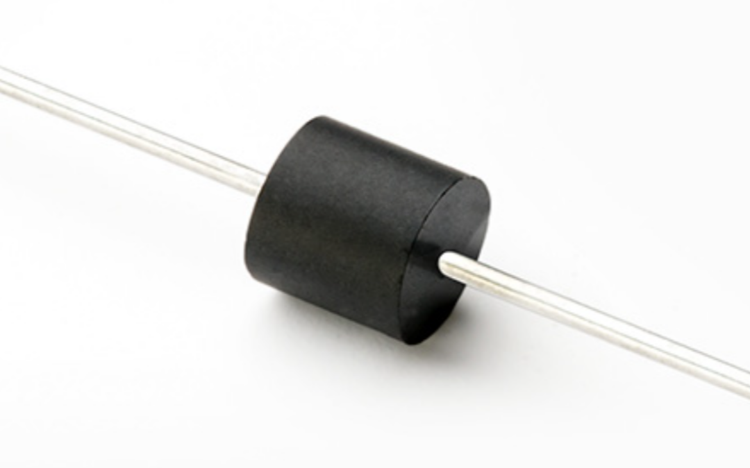
Dedicated ESD Protection Circuits
- Series Resistors: Introducing series resistors in the circuit can limit the surge current caused by ESD, preventing damage to the components.
- Capacitors: Capacitors can be used to absorb transient voltage, helping to protect sensitive parts from high-energy pulses.
- Transient Voltage Suppression Diodes (TVS): These diodes respond quickly to high-voltage surges, clamping the voltage to safe levels and protecting the circuit from ESD.
- Schottky Diodes: Schottky diodes are particularly useful for protecting high-speed signal lines from ESD, as they offer fast response times and minimal impact on signal integrity.
ESD Protection Measures During Manufacturing and Handling
Effective ESD protection does not end with the design phase. In PCB manufacturing, storage, and transportation, additional precautions must be taken to ensure the product is not damaged by static electricity. At JY PCBA, we implement a strict range of measures to safeguard against ESD throughout the entire production process.

Production Environment Protection
- Workstation Grounding: All workstations at JY PCBA are equipped with grounded anti-static mats and wrist straps, with regular checks to ensure the grounding system is effective. This helps to prevent any build-up of static charges during the assembly process.
- Humidity Control: To reduce the accumulation of static electricity, we maintain appropriate humidity levels in our production environment. Proper humidity helps to dissipate static charges, making it harder for them to build up.
Personnel Protection
- Anti-static Clothing: Workers must wear anti-static garments, shoes, hats, and wrist straps, ensuring they are properly grounded during the assembly process. This reduces the risk of transferring static charge from the worker to the components.
- Regular Training: Employees receive ongoing training on the importance of ESD protection and the specific actions they need to take to protect the products. This ensures that every worker understands and follows proper ESD control procedures.
Storage and Transportation Protection
.png)
- Anti-static Packaging: Components and PCBs are stored in anti-static containers and packaging materials to prevent static buildup. This helps to avoid any potential ESD damage during handling and storage.
- Transport Measures: During transportation, we implement strict anti-static measures, ensuring that any electrostatic charge generated by friction or vibration is safely dissipated.
Conclusion
Electrostatic discharge poses a significant threat to PCBs and electronic components, but through careful design, manufacturing, and handling, the risks can be minimized. At JY PCBA, we are committed to providing a one-stop ESD protection solution, ensuring that every step of the PCB production process is optimized to prevent static damage.
We look forward to partnering with you! Click the video below to learn more about our comprehensive ESD protection measures and the services we offer in PCB manufacturing.